![[LWN Logo]](/images/lc.png)
![[Timeline]](/images/Feature.png)
|
|
|
|
|
Weekly Edition Daily updates Events Calendar Book reviews Penguin Gallery |
Making Printed Circuits With PCB
InstallationTo install PCB on your system, download the gzipped source code file, (Netscape users should press shift before clicking), and compile the program. The following steps were performed on a Red Hat 6.2 system with all packages installed:A complete manual and reference card written in PostScript are included in the doc directory. To view the manual, either print the files on a PostScript printer or run gv on the file to view it on the screen. PCB currently has no included man pages.$tar -xzvf pcb-wip.tgz $cd pcb-1.7 $xmkmf -a $make become root and install the program: #make install Exit the root shell and run the program: #exit $rehash $pcb Working with PCBNetLists
Rat's Nest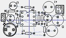 A rat's nest diagram shows which pins are connect together.
Connection lines are drawn with the shortest possible path, so the
appearence is somewhat jumbled looking, hence the name.
After you have labeled all of the parts and loaded the netlist file,
plot a rat's nest diagram by typing 'w'.
The rat's nest can be erased with 'e'.
At this stage, parts should be moved around the page and rotated to minimize
line crossings.
The rat's nest should be created and erased often during this part of the
process.
If there are problems with the netlist file or parts are missing,
the rat's nest operation will pop up useful diagnostic messages.
A rat's nest diagram shows which pins are connect together.
Connection lines are drawn with the shortest possible path, so the
appearence is somewhat jumbled looking, hence the name.
After you have labeled all of the parts and loaded the netlist file,
plot a rat's nest diagram by typing 'w'.
The rat's nest can be erased with 'e'.
At this stage, parts should be moved around the page and rotated to minimize
line crossings.
The rat's nest should be created and erased often during this part of the
process.
If there are problems with the netlist file or parts are missing,
the rat's nest operation will pop up useful diagnostic messages.
Entering Traces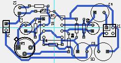 The next step involves running traces between pins on the same node.
Prior to laying any traces, you should click on "sizes" at the top of
the window and pick "adjust" and "use" for at least one type of trace.
The image transfer method shown below requires fairly fat traces, a
0.035" trace width is a good starting point.
The rat's nest shows which pins connect together, traces should connect the
same pins together without overlapping other traces.
In the example PC board, it was possible to make a single-layer board without
using jumpers.
In a single-layer board, jumper wires will be required if traces must cross one
another.
PCB supports multi-layer boards, but the prototyping method shown here
works best with single layer boards.
As the traces are added, the rat's nest should be erased and redrawn to
show where traces are still needed.
When no more rat's nest wires show up, the trace wiring is complete.
The next step involves running traces between pins on the same node.
Prior to laying any traces, you should click on "sizes" at the top of
the window and pick "adjust" and "use" for at least one type of trace.
The image transfer method shown below requires fairly fat traces, a
0.035" trace width is a good starting point.
The rat's nest shows which pins connect together, traces should connect the
same pins together without overlapping other traces.
In the example PC board, it was possible to make a single-layer board without
using jumpers.
In a single-layer board, jumper wires will be required if traces must cross one
another.
PCB supports multi-layer boards, but the prototyping method shown here
works best with single layer boards.
As the traces are added, the rat's nest should be erased and redrawn to
show where traces are still needed.
When no more rat's nest wires show up, the trace wiring is complete.
Filling Empty Space When all of the parts are connected, it may be useful to fill in unused
space on the board with "copper".
I recommend filling the large spaces with rectangles and using the polygon
fill for the smaller spaces.
Filling the "whitespace" with "copper" may improve electrical shielding and
will extend the life of the etchant chemicals.
The "silk" button on the side can be clicked to toggle the parts silk
screen layer, this improves visibility of the copper layer.
After the empty space has been filled, the printed circuit artwork
may be used to build a prototype circuit board.
When all of the parts are connected, it may be useful to fill in unused
space on the board with "copper".
I recommend filling the large spaces with rectangles and using the polygon
fill for the smaller spaces.
Filling the "whitespace" with "copper" may improve electrical shielding and
will extend the life of the etchant chemicals.
The "silk" button on the side can be clicked to toggle the parts silk
screen layer, this improves visibility of the copper layer.
After the empty space has been filled, the printed circuit artwork
may be used to build a prototype circuit board.
PrintingThe artwork should be saved to a file by clicking on "file" at the top of the screen and selecting "print layout". A series of PostScript files will be created, one per layer. The output_group1.ps file contains the bottom copper layer that will be used in making the prototoype. The output_componentsilk.ps file contains the silk screen image that may be used to determine where the parts go.Parts Silk ScreenOptionally, the parts silk screen image may be put onto the component side of the circuit board. To do this, it is necessary to mirror the silk screen image by manually editing the output_componentsilk.ps PostScript file.Find the lines that say: and add a line of PostScript as shown below:%%Page: 1 1 %%BeginPageSetup The silk screen image should be printed onto the transfer material and that should be ironed on to the etched and drilled circuit board. Packing tape should again be used to remove the excess paint from the board. The example circuit board does not have a silkscreen layer.%%Page: 1 1 8.5 72 mul 0 translate -1 1 scale %%BeginPageSetup Producing a Prototype PC Board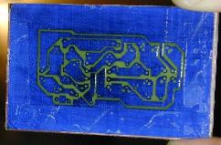 This step involves the use of a commercial circuit board transfer film called
Techniks Press-N-Peel blue.
Techniks appears to be the only source of this type of transfer film.
A PostScript laser printer is required, an ink jet printer won't work.
It is possible to print the artwork on an ink jet printer
and photocopy the image onto the Press-N-Peel film, but some quality
will be lost.
The film works by combining its emulsion with the printer's toner to make an
adhesive paint-like coating that can be fused to a circuit board with heat.
If you are making small boards, you can get several transfers from a single
sheet of Press-n-Peel film.
Print the image onto the paper to get an alignment area.
Cut out an oversized piece of the blue film and tape the leading edge
of the film to the paper.
Run the paper with film through the printer and print the image onto the film.
This technique may not work on all laser printers, proceed with caution
as it could result in paper jams. If your printer has a straight-through
output path on the back, use it.
This step involves the use of a commercial circuit board transfer film called
Techniks Press-N-Peel blue.
Techniks appears to be the only source of this type of transfer film.
A PostScript laser printer is required, an ink jet printer won't work.
It is possible to print the artwork on an ink jet printer
and photocopy the image onto the Press-N-Peel film, but some quality
will be lost.
The film works by combining its emulsion with the printer's toner to make an
adhesive paint-like coating that can be fused to a circuit board with heat.
If you are making small boards, you can get several transfers from a single
sheet of Press-n-Peel film.
Print the image onto the paper to get an alignment area.
Cut out an oversized piece of the blue film and tape the leading edge
of the film to the paper.
Run the paper with film through the printer and print the image onto the film.
This technique may not work on all laser printers, proceed with caution
as it could result in paper jams. If your printer has a straight-through
output path on the back, use it.
The following steps describe the process of producing a prototype board:
Voilà, Instant Hardware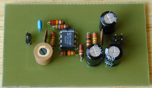
Wish ListPCB's built in parts libraries are rather minimal. There are enough parts defined to do many basic circuits, but adding new new parts to the libraries is difficult. The addition of a graphical parts editor would be a big improvement to PCB. PCB lacks many of the fancy features found in commercial circuit board packages such as automatic parts placement and wire routing. Automatic white space filling would also be a big plus for PCB. While those features are time savers for production work, they are not show stoppers, the program is a very useful tool for the hardware designer.ConclusionPCB is reliable and effective for basic PC design work. It is a good addition to the Linux hardware-hacker's toolkit. PCB could definitely benefit from the addition of more features, it could be a good project for a grad student to work on.It is now possible to produce electronic prototypes in a few hours using only free software. The previously long development cycle for making circuit boards has been greatly shortened. Lessening the time delay means that designs can be iterated more, as in software design, and a better final product can be created. References
author: Forrest Cook, cook@eklektix.com.
|